Brief theoretical information
Time parameters andtransistor characteristicsdetermine and investigate in key mode. Great importance has the switching time , which limits the speed of operation of radioelectronic equipment. This parameter is determinining by the processes of accumulation and dispersal of unbalanced charge in the base,in the collector of transistor ,in the emitter and collector transitions.
When we use a transistor as a key it is in cut-off mode ( closed mode ) or saturation mode . In the first case, in collector circle and the base circle flows small reversed current ICB0, and the voltage on the key output in scheme with the 3E :
UCE = Ec-RcICB0 Ec.
During applying to the input pulse straight current of sufficient importance transistor opens and transfer into saturation mode. Collector transfer voltage UCEsat= Ec -RcIcsatappears to bestraight. Collector transistor opens and starts the holes injenction ( in the transistor pnp type) from the collector in base.Then, in this case, holes are injecting into the base from both transitions - emitter and collector . In saturation mode with increasing input current IBcollector current almost doesn’t increase, increases only carrior charge injection from the collector into the base andin accordance with nonequilibrium base charge. Differential output voltage transistor switch
UBИX = UCEвід – UCEsat= Rc(ICsat - ICB0).
The processes of accumulation and charge dispersal significantly affect on the shape of pulses at the output key. Graphsof voltages and transistor currents during switching shown in Fig. 5.1.
Initially, the transistor is closed with help of source of constant setEB( Fig. 5.1 a)During input rectangular impulse of straight voltage UBX on the circle base flows current IBE,, the value of which is determined by the value of resistance emitter transferrE and resistor in circle base RB.AsRB >>rE, thenIBE= (UBX –EB)/RB.
After finishing impulse (switching voltage of the emitter transition on reverse ) reverse current switch , as in the diode has significant reference value , limited only by resistance in the ring of baseIBE = EB / RB. Emitter transition resistance at first time after the switching is very small because of saturation the base by nonequilibrium carriers of charge . As far the dispersal of nonequilibrium charge reverse resistanse of emitter transition increases and the current base tends to value which was astablished IBE0( Fig. 5.1 b).
With rectangular shape impulse input currentIBimpulse output current Iс(Fig. 5.1 , c)appears with delaytd, which is mainly determined by the duration of the movement injected charge carriers to the collector transition . The delay time is determing by the time interval between the moment,when the input impulse has reached 10 % of its steady-state value, and the moment when the output impulse also reaches 10 % of its steady-state value. After the transistor will switch from the cut-off mode to the active mode , collector current starts to increase gradually , reaching a stable value for the timetr, which is determined by the time interval during which the output impulse increases from 10% to 90 % of its steady-state value , depending on the speed accumulation of nonequilibrium charge in the base and speed of discharge volume of the collector.Thus, the full time switch transistor consists of the delay time and duration of growth:
ton= td+ tr
After supplying the circle base reverse voltage that covers the emitter junction , the output ( collector ) current don’t stop immediately. During some time, the duration of dispersal ts itpractically saves the value because of the concentration of charge carriers in base near collector junction still higher than the equilibrium and the collector as a result of this transition remains open ( Fig. 5.1 c, d ).
Only after the nonequilibrium charge in the collector junction disperse due to release of holes from the base and recombination , the collector current begins to decrease gradually , reaching for the duration tfdecreasing values ICB0. During this time, continuing dispersal of nonequilibrium charge is recharging base and collector junction capacitance . Emitter junction it may close earlier or later depending on the speed of the collector dispersal of nonequilibrium charge concentrated near it.The process of accumulation and dispersal of nonequilibrium charge base qBduring switching transistor shown in Fig. 5.1 g accumulation begins in the interval which is determined by the duration of the delay td. The charge for the rise time trreaches the valueq’B = Qактdue to injection of charge carriers from the emitter junction . Later in the saturation mode the charge base increases due to injection of carriers with both emitter and collector of transitions , reaching values
q’B = Qакт. After the dispersal of nonequilibrium charge base during the time off swiyching off toff = ts + tfthe charge in the base reaches zero.
The values of tonandtoffare determinative in the assessing possibilityof using the transistors in the equipment at a preset speed.
In Fig. 5.1 A shows the oscillogram of voltage pulse , which is formed at the exit key on the BT type pnp.
One of the main problems with increasing speed key is to reduce the time dispersion of the excess charge . To do this , you need to reduce the amplitude of the input signal , and hence the current base (Fig. 5.1 , b), ie - the degree of saturation S = IB/IBsat. But at the same time increases the duration of growth. Moreover, inreal conditions the degree of saturation exceed the minimum value Smin ( thevalue S = 1 corresponds to the border with Active Mode ). Otherwise, a slight decrease in the coefficient knk or transistor base current is transferred to the active mode, and is accompanied by an increase of residual stresses on the key .
A common way to destract transistor saturation and at the same time to avoid marked complications is using in the key of nonlinear feedback. For this purpose between the collector and base of transistor turn on Schottky diode (Fig. 5.2).
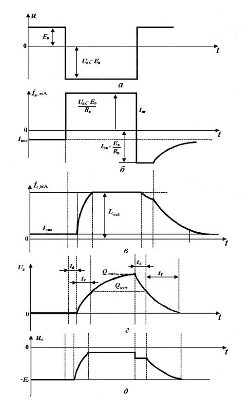
Figure . 5.1. Oscillograms : a-as input ;b -base current; в-the collector current in г- charge basis ;д-A collector voltage of the keys to BT type p –n-p
When the transistor is closed or works in active mode , collector positive potential relative to the base (using transistors npn). Thus , the diode is
situated under reverse off-set has great resistance and does not affect on the work of key. When in the prosses of forming front relative to the potential collector base passes through zero and becomes negative , the diode unlockes and direct voltage is installed on it. If this voltage is less than 0.5V ( which is typical for Schottky diodes ), the collector transition is almost closed , and thus off the modedual injection and accumulation of excess charge , peculiar mode of saturation. As a result, at closing the key there will be nostage of the dispersal of excess and delay downturn. The combination of transistor and Schottky diode is called the transistor with Shottky’s barrier and widely used in integral secuitrytransistor with Schottky barrier and is widely used in integrated circuit design .
It should be underlined that despite of the lack of saturation the key with the Shottky’s barriers is less sensitive to change the coefficient of transfer current B and current which unlocks as the residual voltage little depend’s on these values the delay time and duration of growth are the same as in saturated keys.
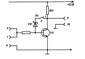
Figure . 5.2. Circuit diagram for the studytransients in BT with the common emitter
References: [1 , c. 92-100 ], [ 3 , c. 99-101 ], [ 4 , c. 135-138 ], [ 14].
Order of work.
Research temporal characteristics and parameters of bipolar transistors in switch with CE and WB performed using the scheme shown in front module 4 "Study of transients in bipolar transistors " (Fig. 5.2 and 5.3). It is necessary befamiliarto the wiring diagram module and it’s location on the panel of regulatory elements. Connect the transistor,which is investigating to the corresponding terminals of the module "E -B -C ."
1. Explore temporal key on the BT scheme according to a common emitter scheme. To do this:
- SA2 transfer switch in the down position " OM " and SA3 - in the up position "I" ;
- Turn on the stand and power supply variation of 12 V.
2. Turn on the oscilloscope and its input amplifier " In -II" connected to terminals 9 and 10.
3. Set to " ~" (open for DC input ) switch input on the front panel of the oscilloscope .
Potentiometer "  " , located on the top right corner of the module 3, set the voltage at the collector 10 V (measurement makes oscilloscope ). The transistor must be in cutoff mode
  .
.
4. Switch on pulse signal generator and its synchronization pulses tosynchronizea sweep of the oscilloscope. When using a generator G5 -54 set the following modes: press the start button , set the frequency 100 kHz, time shift - about 1 ms, pulse duration - 3 ... 5 microseconds, the positive polarity - «__ «. A test signal output via the output of 1:1 (the button is "X 0.03 "). Connect the generator to the terminals 6 and 8 on-board of laboratory module.
5. Determine the minimum amplitude of the input pulse Uвх.satthat provides key mode switch saturation. To do this:
- Gently rotating the rotary pulse generator amplitude , to observe the change of the output signal . In the uplink , the key is in cutoff mode and UC = EK. Peak output negative pulse with increasing amplitude of input signalapproaches to zero (UCsat ® 0). An indication of the mode switch key is consistency saturation output amplitude with a further increase in the amplitude of the input signal. Peak pulse modesaturation reaches level UC 0 ( the position of the oscilloscope sweep during switching off it at the entrance of the terminals 9).

Figure . 5.3. Circuit diagram for the studytransients in BT with WB
6. Measure thedelay time delay of output signaltd. To do this:
- Set the oscilloscope sweep time 0.1 ms / cm,the handle ofsmooth adjustment of the sweep turn it clockwise until the end;
- Submit the input pulse amplitude Uвх= Uвх.sat ;
- Using an onebeam oscilloscope its input firstly connect to the terminal7 and fix the position of the leading edge of one of the vertical lines ( use the handle of horizontal displacement oscilloscope "«",, or drum smooth regulation of temporary displacementof synchronous generator) . Then connect the oscilloscope to the output of the circuit. The beginning of the output pulse will be replaced relatively marked by the vertical line scale grid. Given the duration of the sweep and the size of the displacement output pulse relative to the input horizontally , determine td;
- Using a two-beam oscilloscope input connected to the input circuit 7, a second input - to exit 9. On the same time, there are two impulses on the screen. Potentiometer "  " align them vertically. By shifting the leading edge of the output pulse relative to the input horizontally, taking into account the duration of the sweep determinetd. For a more clear determination of the borders of the leading edge of the input and output pulse attenuator amplifier oscilloscope should be transferred to the position 0.2 V / cm and 1 V / cm.
7. Measure the rise time , dispersal and decrease output pulse during its duration about 3 ... 5 microseconds. Time dispersion measure for the duration of the sweep oscilloscope 0.1 - 0.2 ms / division . The momentum shift in the center of the screen handle «. Draw the output waveform , noting the drawing level and zero potential.
8. Investigate the improving speed of key,with the help of a nonlinear feedback. To do this:
- Connected between the collector and base of transistor diode VD ( SA1 transfer switch in position " 2") ;
- Submit the input pulse amplitude Uвх=0,5Uвхsat. Draw oscillogramand compare oscillogram withobtained for a given value of the amplitude of the input signal in Section 7. Compare theoscillogram of the output pulse oscillogram when connecting and disconnecting the diode VD ( when switching the switch into position "2" );
- Submit the input pulse amplitude Uвх=1,5Uвхsat; define a dispersal time ts and sketch the output waveform in twoswitch positions ( when connected and disconnected diode );
- Assess thethe improving speed of key,with the help of a nonlinear feedback;
- Turn off the power supply unit of 12 V.
9. Explore temporal key options on the bipolar transistor during swiching off the scheme with a common base . To do this:
-transfer switch SA2 in the up position "SB " and SA3 – to position " 1";
- change the polarity of the pulse generator ( theinvestigating of n-p-n transistors in the emitter circuit is fed negative pulse );
-display in the left extreme position potentiometerUE ;
- switch power supply unit 12 V;
- Measure the elapsed time delay, the growth, the dispersal ts and decreasing tf according to the methodologydescribed in Section 6.7 . The duration of input pulses can be reduced to 1 ms, and the amplitude should be increased.
10. Compare the speed of key using schemes of bipolar transistors with common emitter and common base .
11. To investigate the dependence of the amplitude of the output signal of the voltage cutoff UE.To do this:
- Sketch waveform and determine the amplitude of the output signal when applied to the input pulse 0,5Uвхsat, Uвхsatand 1,5Uвхsatat three positions potentiometer UE( two extreme and one medium ).
12. Turn off appliances, power supply unit and stand.
13. Formulate conclusions , to report.
Contents of the report
The report should contain:
1. The purpose of laboratory work.
2. Oscillograms of the input signal base current, collector current , unbalanced charge in the base and the collector voltage of the keys to bipolar transistors with common emitter .
3. The principal electrical circuit using bipolar transistors keys with CE and WB to investigate transients.
4. Results of experimental studies of key schemes BT in the form of tables and oscillograms of the output pulses .
5. The findings, based on an analysis of the results.