TCAD-Driven ESD Optimization
TCAD for Electrostatic Discharge
Introduction
Electrostatic discharge (ESD) is a major threat to the reliability of integrated circuits, where approximately 20% of total integrated circuit (IC) failures are due to ESD [1]. Discharge of charged objects or human discharge into IC chip pins with very high currents (up to10 A) and short duration (1 ns to 200 ns) causes serious damage to the very sensitive devices of the circuitry. This happens during manufacturing, assembly, shipment, and in thefield.
This article demonstrates the successful use of TCAD for the simulation and investigationof ESD-related problems, as well as for the development and optimization of ESDprotection devices and methodologies withrespect to ESD robustness. The full range fromESD calibration, ESD device simulation, toESD compact modeling for circuit simulation is covered.
Background
The operational regime of devices underESD stress is far beyond the range of normaloperation conditions. Among the most important effects to be considered within theESD regime are self-heating, conductivitymodulation due to high carrier injection, nonuniform operation (current filamentation),and avalanche breakdown at reverse-biasedjunctions.
To characterize the device high-currentregime, mostly the transmission line pulsing (TLP) technique is used [2]. This two-terminaltechnique consists of feeding a constant current pulse into the device under test (DUT)and monitoring the voltage response. Thepulse has a typical duration of 100 ns with arise-time of 10 ns. The characterization usingTLP allows for obtaining device characteristicsup to very high current levels, while preventingearly destruction due to self-heating.
Within the device simulation environment,TLP is used to calibrate high-current, hightemperature regimes to measurements. For the qualification and specification of ESD robustness, other more realistic ESD stress models are used. The most prominent one is the human body model (HBM), which reproduces the discharge of the body of a human being. Additional models used are the machine model (MM) and the charged device model (CDM). Apart from the field of application, they differ from the HBM due to a different rise-time, peak current, duration, and polarity [3].
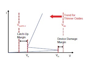
In summary, the basic functionality of an ESDprotection device or circuit is to provide a low-resistivity discharge-current path, which prevents the internal circuitry as well as the protection device/circuit itself from being damaged during an ESD event. The ESD protection functionality is ‘transparent’ to the internal circuitry under normal operation conditions. Figure 1 shows the most important parameters of the so-called ESD design window.

«Fig. 1.» Typical ESD design window for protection devices.
TCAD-Driven ESD Optimization
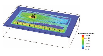
TCAD is a powerful tool for identifying and investigating ESD-relevant effects, providing insights into the internal device behavior (such as temperature and current distributions, and electric fields) under ESD stress conditions, which are generally not accessible by measurement. In particular, TCAD can be used successfully for the study of 3D effects arising from device layout or inhomogeneous current flow as shown in Figure 2. TCAD is invaluable for modeling these complex ESD effects [4][5], providing

«Fig. 2.» Formation of current filament leading to temperature hot-spot in a device during an ESD pulse using Sentaurus Device 3D device simulation.
simulation results that complement expensive measurements and reducing expensive experiments on wafers.
From the device or TCAD engineering perspective, establishing a full-fledged ESD TCAD workbench from process and layout information, and from the calibration of simulation models including the high current/high temperature regime, allows the evaluation of process variation influences, thedetermination of layout dependency, and the optimization of ESD structures. The improved understanding of the internal device failure modes results in building better input/output protection structures and the possibility of virtual testing and development of new structures. TCAD also helps speed up ESD design to keep pace with IC developments at reduced design-cycle times by reducing time-to-market and cost-to-market.
From the circuit or library design perspective, TCAD permits the development and application of physically based SPICE ESD compact models and parameter extraction methodologies from simulation and measurement. The SPICE ESD compact models allow for simple and fast use within circuit and analog design, and for optimization of protection configurations. The simulationbased methodology allows checking of critical input/output protection configurations before IC tape-out and avoiding redesigns.