INVESTIGATION OF TRANSITIONAL AND FREQUENCY PARAMETERS OF SEMICONDUCTOR DIODS
Laboratory work 2
Purpose of work: To deepen and consolidate knowledge about basic processes taking place in semiconductor diodes (SD), about their peculiarities as elements of electronic circuits, the limit operating parameters and characteristics of such devices in the dynamic mode. SD Study in pulse mode, straightening and limiting voltage. Acquiring the skills of the experimental study of transient processes, frequency parameters, rectifying properties and determination of performance SD.
1. Brief theoretical information
Basic properties of semiconductor diodes.
Electron-hole transition, except the effect of rectification, has other properties (nonlinearity of current-voltage characteristics, barrier capacitance), they also possess striking phenomenon of ionization of atoms of the semiconductor in the reverse, so in certain circumstances and with a direct switching on. These properties of p-n junction is used to create different types of SD: rectifier diodes, stabilitrons, varicaps, photodiodes, light diods.
Using the rectifying diode rectification effect is achieved due to large difference of resistances during the injection and extraction of charge carriers (at direct and back switch). The most widely acquired are germanium and silicon diodes, also Schottky diodes, that use the metal-semiconductor contact (as rectified).
It is important to remember that silicon diodes at reverse switch have on six orders smaller value of thermal current Io, than germanium, due to a lower concentration of majority carriers, due to the width of band gap (1.87 eV in silicon, 1 13 eV in germanium). For the same reason direct line VAC in silicon diode goes to the right from germanium (shift by 0,25 ... 0,35 V) (Fig. 2.1).
Choosing the type of diode it should be taken into account its operational boundary data: average rectified current, reverse voltage (amplitude value), operating temperature range, relative humidity, pressure, vibration, constant linear acceleration, operating time warranty.
Full list of parameters of SD is contained in the state standard of Ukraine "ISO 2332-93". Semiconductor diodes. Terms, definitions and literal signs of electrical parameters, then it is used designations recommended by this document.
For the calculation of circuits, containing diodes and their modulation it is used the following parameters: resistance Rp differential resistance r by current, differential steepness of VAC S and full capacity of diode Ctot =Cj +Ccast,where Ctot value of capacitance between the diode conclusions in set mode; Ccast – value of capacity between diode body conclusions due to absence of a crystal.
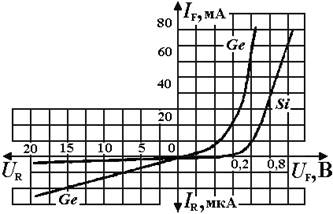
Fig. 2.1. VAC of diodes at  :
:
Ge - germanium diode ID507A;
Si - silicon diode 2DI03A
For the calculation of circuits, containing diodes and their modulation it is used the following parameters: resistance Rp differential resistance r by current, differential steepness of VAC S and full capacity of diode Ctot =Cj +Ccast,where Ctot value of capacitance between the diode conclusions in set mode; Ccast – value of capacity between diode body conclusions due to absence of a crystal.
In the area of high frequencies starts to show inertia movement processes of charge carriers, and therefore it is used dynamic models of diodes.
With rapid change of diode voltage, oscillation period becomes comparable to the time of accumulation and dispersal of nonequilibrium carriers in the base and not volumetric charge in an electron-hole transition. It creates a dynamic mode. In this mode it is necessary to take into account the capacitive properties of the diodes, their ability to accumulate and to give the charge with increasing or decreasing of the applied voltage. Charge accumulation occurs in the p-n junction and in the basis of diode. Under this there are two components of capacitance diode Cj: barrier Cbar and diffusion Sdf. Thus Cj = Cbar + Sdf. In back switch of diodes, as well as at a direct low voltage charges are accumulated directly on the edge of p-n junction. Inertia of their accumulation and dispersal are taken into account by barrier capacitance. Increasing the reverse voltage increases the thickness of transition, facing of capacitor and its capacitance decreases. Dependence of diode capacitance on the applied voltage is used to build a special SD-varicaps. They are the capacitors, capacitance of which depends on the reciprocal of the voltage and is determined using VFC Sbar = ƒ (UR).
The transition in direct voltage central role played by high-signal accumulation processes non balanced charge in the database, using the model of diffusion capacity. At the analysis of circuits in described modes, diodes should be submitted as a dynamic model (Fig. 2.2), where L - inductance of diode; Ccast, Cbar, Sdf - capacity of building(body), barrier and diffusion capacity of junction; r, Rp, rv, - resistors that determine the differential resistance and variable resistance of p-n junction, and resistance of the diode base.
Inductance of diode consists of inductances of outputs and contact spring, which connects the crystal with one of the terminals.
Capacitive properties limits the speed of action pulse or key diodes. Time dependences of voltages and currents that characterize the transition processes in semiconductor diodes, depend on the amplitude of signal (density of direct current) and from resistance of external circuit, in which diode is connected. Therefore it is necessary to consider four cases of transitional processes.
Transient processes at high voltages and currents.
With relatively high density of direct current, which passes through the diode, accumulation of minority carriers in the diode(diffusion capacity) plays the primary role.
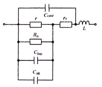
Fig. 2.2. The dynamic model of the diode
Let`s consider the transition processes in connecting of diode to the voltage generator (r <Rh). When a diode is submitted by direct voltage pulse (Fig. 2.3 a) the diode current reaches a constant value not just because the initial moment of resistance of the diode continues to be great. With time, in the basis is accumulated injected through p-n transition minority carriers. As a result, resistance and voltage drop on the base are reduced, and on the p-n junction - increase, causing the increasing of the injection. Diode current increases gradually to stable value. After the impulse finishing, to the diode with jump reverse voltage is submitted (negative bias voltage Esh). Switching diode from direct to reverse voltage at the initial point there is a high reverse current, limited mainly by consistent resistance of base. This current is caused by minority carriers, accumulated in the base. Reverse current keeps its value during the time of dispersal (td). Then, all accumulated carriers in pass through the p-n transition or recombine in the diode base, as a result, reverse current decreases to a stationary value – saturation current. At that time recovery of diode reverse resistance ends.
The process of dispersal of accumulated carriers is much slower than the process of their accumulation, therefore the process of dispersal determines the frequency properties and speed of action of most diodes. For pulse diodes there is a parameter of length reversion trr – duration of recovery reverse resistance or current, which is determined by a time interval between the moment of voltage switching on diode from direct to reverse and a moment, when the reverse current drops to this value (Fig. 2.3 a).
During the connection of diode to current generator (r <<Rh) current, passing through the diode, coincides by the form with pulses of generator (Fig. 2.3, b). In this mode voltage pulses are investigated on the diode. During passing of direct current through the diode for the first time after switching on, there is the rise of voltage. This is caused by a great initial resistance, which is kept for as long as the injected carriers do not reduce the base resistance of the diode. Therefore, to evaluate the performance at connection of pulse diodes to current generator it is used parameter – duration of diode direct restoring tfr. This is an interval of time during which diode is switched on and direct voltage on it is set from the value, equal to zero, to the given steady-state value.
Normally this parameter is fixed at a level when after the maximum emission voltage drops to a value of 1.1 ... 1,2 U (see Fig. 2.3, b).
Transient processes at low voltages and currents. When applying to diode small direct voltage (work with voltage generator) modulation effect of base thickness and resistance due to low injection level is very small (Fig. 2.4 a). Therefore, diode resistance has a capacitance character. Current which passes through the diode increases sharply and is limited only by resistance of base.

Fig. 2.3. Oscillograms of currenst and voltages of pulse diode during its work
in mode of high amplitudes in schemes with voltage generator (a) and current
generator (b)
In the process of charging of the barrier capacitance voltage on p-n junction and current through the diode tends to some set of values that are defined by the active component of p-n junction resistance. At the time of diode switching, the voltage on barrier capacitance can not change instantaneously, it reaches a steady value after some time. The diode current has a negative release and gradually decreases (Fig. 2.4 a).
During connecting of current generator in the first moment of pulse act whole current consists of capacitive component. Therefore, the voltage on the diode is determined by voltage drop on the base resistance of diode (Fig. 2.4, b). In the process of charging of barrier capacity, voltage on the diode increases. For diode switching off, on it there is residual voltage, which decreases with time (Fig. 2.4, b), which is determined by discharge of capacity through the active resistance of p-n junction.

a b
Fig. 2.4. Oscillograms of currents and voltages of pulse diode
During its work in low-amplitude mode in the schemes with
voltage generator (a) with current generator (b)
For diodes, developed after 1964 there is given marks of four elements: the first element-letter or number, that indicates the output material (G or 1 - germanium, S or 2 - silicon, Ga or 3 – gallium compounds), the second element - the letter that indicates the subclass of device (V- varicaps, R - rectifying universal and impulse, C - rectifying columns, blocks, etc..), the third element - the number, the first digit of which indicates the classification number and the next two digits (from 1 to 99) – order number of development (except stabillitrons and stabistors). For each type of semiconductor diodes there is installed its own classification number (varicaps - 1,2; rectifying blocks depending on power - 3,4; rectifying diodes of low power (direct current until 0,3 A) - 1, average power (direct current from 0,3 to 10 A) - 2. Pulse diodes are classified by the duration of reverse resistance recovery: more than 150 ns - 5, from 30 to 150 ns - 6, from 5 to 30 ns - 7, from 1 to 5 ns - 8 ns less than 1 - 9. For example, KD504A - silicon diode, pulse, with recovery time more than 150 ns.
Diode conditions of exploitation are given in the handbook [4, 8]. You must remember that to increase the reliability of workloads of diodes should not exceed values higher than 70-80% of limit.
Literature: [1, c. 14 - 39, 44 - 49], [2, c. 4 - 19], [3, c. 19 - 44];
[4, c. 94 -99], [5], [7].
2. Order of work execution
Work is performed using laboratory module 1 "Study of semiconductor diodes.
1. Study electrical schematic for investigation of transient and frequency parameters of semiconductor diodes, with appointment of switches and sockets on the board (Fig. 2.5).

Fig. 2.5. Circuit diagram for the
semiconductor diodes study
2. Explore the transition processes in semiconductor diodes D226, D223B and D2ZH with voltage generator in large amplitudes mode. To do this:
- switch on pulse generator and two-beam oscilloscope;
- connect the output of the generator 1:1 to pins of removable board 1 and 3 laboratory bench;
- set using buttons and handles of smooth adjustment such a parameters of input test signals: frequency - 100 kHz, the length of delay - 0,5 ms, pulse duration - 0.6 ms, the polarity - positive, the amplitude - 1.0 V;
- connect output of synhro impulse generator to input SYNCHRONIZATION of oscilloscope. Switch SYNCHRONIZATION of oscilloscope put in position EXTENAL and using the handles LEVEL and STAB achieve the sustainable state of oscilloscope development and its absence at switching off at generator synhro impulse;
- connect one oscilloscope output to the input of circuit (terminal 2) (or to the output of the generator), and second - to the output of circuit (terminals 6 and 5 – BOARD);
- with switch DEVELOPMENT set a duration, which will provide display of pulses so, that the oscillograms occupied 1 / 3 ... 1 / 4 of the oscilloscope screen;
- connect diodes D226, D223, D2ZH to the board and measure duration of dispersion and duration of reverse resistance recovery trr;
- set the class of semiconductor diodes D226, D223, D2ZH by the duration of reverse resistance recovery.
3. To investigate the frequency properties of diodes D26, D223 and D2ZH. To do this:
- turn on the generator of harmonic oscillations. Set the following parameters of sinusoidal oscillation: frequency 200 kHz, amplitude up to 1,5 V (to put switch in position "1.5");
- connect the output of the generator of harmonic signals to the input of board (to turn off the cable from the output of pulse generator and connect it to the output of the generator of harmonic oscillations);
- transfer the switch in position of oscilloscope SYNCHRONIZATION to position INTERNAL I. With oscilloscope switch DURATION OF DEVELOPMENT set such duration, in which it displays 4 ... 5 junctions of sinusoidal input signals;
- connect the next oscilloscope to the terminal 6. Switch "SA" on-board of laboratory stand put into position "2". Thus, diodes are investigated in the rectifier circuit;
- draw and define the amplitude of positive and negative one-half period at frequencies 200 Hz, 2 kHz, 20 kHz and 200 kHz. Frequency set is achieved by the switch FREQUENCY MULTIPLIER of generator ;
- make conclusions about the use of diode for rectifiers building in the frequency range of 200 Hz - 200 kHz.
4. Explore diode D223 in the scheme of limiting amplitude. To do this:
- transfer switch "SA" on the board to "1", the second input of oscilloscope connected to terminal 4 (terminal 5 BOARD) and using the potentiometer "↕" of second oscilloscope input combine the development with central line of oscilloscope screen;
- remove the dependence of the positive half-amplitude (count from the center line of the screen at position of amplifier switch of second channel oscilloscope 0.5 V / Div). By changing the input signal amplitude in range from 0.1 V to 1.5 V. Build characteristic Vout = f (Vin).
5. Turn off devices.
6. Formulate conclusions and make a report.
3. Content of report
The report must contain:
1. The purpose of the laboratory work.
2. Circuit diagram for the transient processes study in semiconductor diodes at operating in the schemes with current generator and voltage generator.
3. The main parameters of diodes D223 and D226 are taken from listing, with details of their designation.
4. Oscillograms of transients processes in diodes at operating in the schemes with the voltage generator and current generator in the modes of large and small amplitudes.
5. The results of investigations in form of tables and graphs.
6. Conclusions, which are based on analysis of the received results.
4. Control questions and tasks
1. What parameters of diode determine its performance as a key?
2. By what speed of act is limited in diodes?
3. What determines a duration of reverse resistance recovery in diode?
4. Point the classification of diodes corresponding to time of reverse resistance recovery.
5. What diodes are called key diodes (main) ?
6. Explain the properties of diodes properties.
7. Explain the oscillogram of current, flowing through the diode operating with voltage generator using large amplitudes mode.
8. How does the current form, which flows through the diode, at amplitude increasing of input pulse and voltage shift, change?
9. Explain the voltage oscillogram of diode operating with current generator using large and small amplitudes mode.
10.Why do it lose Valve properties at increasing of diode frequency?
11. As a result of what processes does the limiting of pulse amplitude occur?