DIGITAL INTEGRATED CIRCUITS
Laboratory work 8
INVESTIGATION OF DYNAMIC PARAMETERS
DIGITAL INTEGRATED CIRCUITS
Purpose of work:To deepen and consolidate the knowledge about the structure, principle of operation, characteristics and basic dynamic parameters DIS executed in CMOS transistors, skills acquisition experimental determination of the basic dynamic parameters such as DIS K561LA7.
- Brief theoretical information
Features integrated logic elements (ILE) mode switch is evaluated by means of dynamic parameters which determine the reaction scheme in effect at the time of input signals. This the time relationship between input and output signals and time diagrams of different modes of IC.
To dynamically include the following parameters (Figure 8.1):
t1,0 (tTLH) - a transition from the state of IMS logical unit to logical zero state. This length of time for which the output voltage of the IC varies from level log. 1 of the log. 0, measured at 0.9 and 0.1 or the set values of voltage;
t0,1 (tTLH) – a transition from the state of IMS log. 0 in the status log. 1. This length of time for which the output voltage changes from IMS log level. 0 to level log. 1, measured at 0.1 and 0.9 or the set values of voltage;
t0,1затр.(tDHL) – the delay of tern on IC. This is the time interval between the input and output pulses by changing the output voltage of the voltage IC log. 1 Voltage log. 0, measured at 0.1 and at a given level voltage;
t0,1затр.(tDHL) – the delay of tern off IC. This is the time interval between the input and output pulses by changing the output voltage of the IC level log. 0 to level log. 1;
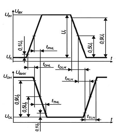
Fig/. 8.1. Dynamic parameters DIS
t1,0 затр.пош.(tPHL)– the delay spread of the signal when you switch IC. This is the time interval between the input and output pulses by changing the output voltage of the IC level log. 1 of the log. 0, measured at 0.5 or the set values of voltage;
t0,1затр.пош.(tPLH) – the delay spread of the signal when turning the IC. This is the time interval between the input and output pulses by changing the output voltage of the IC level log. 0 to level log. 1, measured at 0.5 or the set values of voltage;
t0,1затр.пош.с.(tPAV) - the average delay time of signal propagation logic IC. This interval of time equal to half the sum of the signal propagation delay when you switch and signal propagation delay to halt logic IC:
 .
.
Average propagation delay time determines the speed of DIS. Its value in nanoseconds for different series IC are given in Table 1.
Table 1
| Type logic | р-MOS | KMOS | TTL | ESTL | n-MOS | (  ) )
|
| tPAV | 15 – 50 | 1 3 | 0,5 – 2 | 40 – 100 |
Restrictions on speed, typical for the p-channel MOS circuits eliminated by using n-channel MOS structures. The mobility of electrons in silicon is greater than the hole mobility, providing speed switching MOS circuits with n-channel 2-3 times greater than the schemes of p-channel. Using ion implantation and structures with depleted, not enriched with channels has reduced the supply voltage of 5 V, which makes the scheme compliant for electrical levels of TTL.
A number of important elements have positive qualities injection logic ІЛ2, which appeared as a result of improved technology and circuit design of integrated circuits .
Methods of measuring the dynamic parameters of cis based on the determination of time interval between two different ( or the same ) voltage levels of the input and output signals. For this purpose the pulse generator signal and time interval . In laboratory work to measure time intervals using an oscilloscope.
When measuring the dynamic parameters of the load using the chip and its equivalent.
In logic circuits using MDN transistors with dielectric oxidative  – MOS transistors. The basis of the MOS-transistor logic (ILO TL) are MOS transistor switch inverter. In the key of dynamic loads using transistors with a channel of the same type as in the active transistors. This DMON-transistor logic with a key of the same type of conductivity.
Transistor of the opposite conductivity type channels are performed complementary keys that form the basis of logic CMOS or CMOS TL.
Feature of integrated logic elements in MOS transistors is no current in the input circuit. As a result, the logical level UO and U1 do not depend on the load and remain the same as at idle . The impact of the following key only leads to an increase in the output capacitance of the logic gate.
In Fig. 8.2 shows two typical options ILE MOS logic performed on MOS transistors with n- channel . Using a dynamic load reduces the area ILE and extends one of the main advantages of MOS TL - a high degree of integration. This advantage is due to the fact that the MOS structure does not require special insulation between ILE , unlike structures based on bipolar transistors.
Transistors VT1 and VT2 are active and transistors T3 - dynamic loads. Shutter VTZ connected to drain, then  , i.e.
  – threshold voltage) This means that VTZ working on sloping site. If VT1 and VT2 valves (Fig. 8.2 a) apply voltage U0вх<U0 transistor VT3 enters the open state, its residual voltage is low and U1вих=EC. If the gate VT1 VT2 or apply voltage U1вх <U0 (or both valves), a transistor (or both) enters the open state, the residual stress is small and U0вих→0. Voltage applied to a disabled completely when loading transistor VT3. To reduce the residual stresses in the key of dynamic load transistors VT1 (VT2) and VT3 should differ. In the active transistor width to length ratio of the channel should be as great as in when loading - as small as possible.

Rice. 8.2. Logic elements MOS TL with a dynamic load:
a) perform a logical OR function – NO function;
b) to perform a logical AND function – NO function
Transistors VT1 and VT2 (Fig. 8.2, a) are turned on simultaneously, vidpyrannya each of them leads to a decrease in output level, ie, the circuit performs the logical function 2 OR - NO. When noted above geometry transistors residual stress has the same small value (0.05 ... 0.15 V), as in bipolar keys. Therefore we can assume U0вих = Uзал = 0,1V.
The applicable MOS TL residual stress is reduced in proportion to the number of open logic transistors, as a parallel connection of transistors increase the equilibrium ratio of the width to the length of the channel.
Sure voltage in MOS TL elected 3-4 times greater than the threshold voltage. Therefore, if  = 1,5...3 V, a logical difference (5 ... 10 V) is much higher than the values inherent in schemes DTL, TTL and ІЛ2.
Another advantage of MOS TL is increased noise immunity. To open the required voltage of the transistor is close to the threshold, ie 1.5 ... 3 V, while in bipolar ILE it is 0.7 ... 1.4 V.
Shown in Figure 8.2, to ILE different sequential switching logic transistors. Therefore, in terms of current and low output voltage  possible only when you open all (in this case both) logic transistors. It takes place at the level of feed U1вх all logic inputs. The following ILE functions as 2 AND - NO. level
  in this scheme is the same as in the previous one, but the level of
  more - it is proportional to the number of logic transistors in series enabled and can range 0.2 ... 0.5 V or more. According smaller the logical difference.
Performance MOS TL speed limited recharge capacity СО = ССВ + СЗВ + СМ (паразитна ємність мантажа).Такі ІЛЕ менш швидкодіючі, ніж біполярні.
( parasitic capacitance mantazha ). Such ILE less speed than bipolar .
Logic elements in complementary keys are shown in Fig. 8.3, a and b . The main advantage of CMOS logic is that the change of the output voltage is not associated with a change in current flow : it is close to zero . As a result CMOS logic elements consume very little power. In CMOS structures TL parallel connection of transistors of the same type is accompanied by series connection of some type. Logic function performed is determined by switching transistors " lower" floor. Transistors VT1 and VT2 - transistors inducedn-channel (enriched type) and VT3 and VT4 - with p-induced channel.
If the diagram (Fig. 8.3, a) for both logic input is low level U0вх < , then VT1 and VT2 closed (no channels). As transistors VT3 and VT4 formed channels as voltage and greater than (modulo) the threshold voltage. However, because the flow through the channels of small currents of transistors VT1 closed and VT2, voltage drop across the channel transistors VT3 and VT4 goes low. Therefore, we can assume that the input voltage is equal to the supply voltage U1вих = EC. According logical difference is  .
.

Figure. 8.3. CMOS Logic TL elements:
a) perform a logical OR function – NO function;
b)to perform logic AND function –NO function
Consider the case when the input information signal U1in> U0 served only one input A. This will provide a switching transistor VT1 open. It should be noted that for the normal functioning of ILE on the basis of CMOS structures, input level should be such that the condition is performed. 
Then switching transistor VT4 is provided in the closed state and output logic zero level is formed. Similar processes occur when U1in apply only to input B or on both inputs at the same time.
Output voltage varies with ILE filing of U1in on any of the inputs (A or B) or on both inputs. This element performs a logical function or – no.
State of the diagrams (Fig. 8.3, b) changes only at the level of feed U1vh> U0 at the same time on both inputs. Thus the logic function implemented AND- NO.
In addition to high efficiency, additional advantages CMOS TL compared to MES TL is a small working voltage (up to 2 or less) and higher speed. The last reason is that in such ILE output capacitance is charged and discharged currents open transistors.
References: [1, c. 117-119], [4, c. 223-230], [6], [11], [12], [13], [14].
The order of work
This laboratory work is carried out by means of removable board 8 "Investigation of the dynamic parameters of DIS." We study the integrated circuit K561LA7.
1. See the circuit diagram of the module (Fig. 8.4), with the location and purpose of regulatory elements in the panel. With potentiometer R4 (panel labeled Uin) is installed state of the circuit. In the left extreme position at the gate of the transistor active set U0in<U0. Potentiometer adjusts the supply voltage of +6 V (far left) to + 9 (far right).
2. Dynamic parameters of digital circuits is measured by a generator of rectangular pulses and two-beam oscilloscope. Oscilloscope connected as follows: one input to input 2 or directly to the generator, a second input - output to 4 body - to exit 5. In external synchronization mode via optional cable output sync generator is attached to the synchronization input of the oscilloscope.
3. Turn the stand, power supply 12, a generator and an oscilloscope. LOGIN switches both channels on the front panel of the oscilloscope switch to the "~" (open-input for direct current). Sync transfer switch in position outside and handles level and stabilize. achieve stable synchronization pulse generator (if you disable the sync cable from the oscilloscope sweep should disappear).

Picture. 8.4. Scheme module for laboratory research
dynamic parameters DIS
4. Put hendle potentiometer Uin to the far left , that is set at the inputs <. In this case, the output is set , allowing for an oscilloscope to measure the voltage of the power supply. This strain exhibited a potentiometer . In the study of circuits K178LA7 or K561LA7 must put = 9 V. Scan oscilloscope with increasing voltage is shifted up. On the oscilloscope mark level = 0 and = 9 (at zero scan shifts or by turning off the oscilloscope from the output 4, or by transferring the INPUT switch to the " ~" (closed input VAC )).
5. Explore the scheme to implement logic functions AND - NOT:
- At the leftmost position potentiometer R4 to fix the position of the sweep of the oscilloscope ();
- By turning clockwise R4 set at the entrance>. In this scheme should go to the open position. Scan oscilloscope abruptly moved to a level that meets U0out.
Recorded in the minutes of this level.
6. Determine the threshold value of the amplitude of pulse signals, which provide switching IC mode cutoff and saturation regime:
- Connect the generator to square wave outputs 1 and 3. Set the amplitude of the pulse 2 ... 4 V, duration 1 - 2 ms, repetition frequency - 100 kHz;
- Transfer scheme in cutoff mode (  ) by setting the potentiometer R4 to the far left;
- To establish a positive polarity pulse generator output and increasing their amplitude to achieve the appearance of negative pulses at the output. Fix the value of the amplitude of the input pulses and draw 2 ... 4 oscillogram of the output pulses in the range of significant changes in the shape of input pulse.
Carry potentiometer R4 to the right extreme position and apply the input pulses of negative polarity.
To conduct the study, as in the previous case.
7. Measure the length of the transition from the state of IMS logical unit to logical zero state (  ), a transition from a state of IC logic zero to a logical unit (
  ), the delay enable (
  ), disable the delay (
  ), the delay spread in vimknenni (
  ), and shutdown (
  ). To do this:
- Potentiometer R4 to transfer to the far left;
- Submit to the inputs of an integrated circuit pulses of positive polarity with the parameters listed above, with the inlet shall be generated pulses of negative polarity. Channel oscilloscope connected to input 2, reproduces the input pulses of positive polarity;
- Using an oscilloscope handles the first and second channels combine to screen incoming and outgoing signals. Their size vertical and horizontal time scale (duration of the sweep) set such that it was convenient to carry out the measurement. Use the slow delay adjustment on the front panel of the generator can change the position of the pulse under study relative to the beginning of the sweep using external synchronization (see paragraph 3);
- Draw oscillograms of pulses in the protocol, to measure time intervals mentioned above and apply the values obtained in the oscillogram (see Fig. 8.1).
8. Determine the average propagation delay time ILE.
9. Off gauges, power supply and stand.
10. Analyze the results. Formulate conclusions and make a record of the report.
3. Contents of the report
The report shall include:
1. The purpose of laboratory work.
2. Conditional graphic, schematic diagrams and dynamic parameters of the integrated circuit (K561LA7) under research is obtained from.
3. Scheme of the laboratory module for measuring dynamic parameters DIS.
4. Time diagrams of the input and output pulses (specify dynamic parameters obtained during experimental studies).
5. The research value of the threshold voltage and dynamic parameters in tables and oscillograms.